Multiphase Divide-by-Two CMOS Frequency Divider in Cadence GPDK045
A technical examination and simulation analysis of the 8-phase divide-by-two frequency divider proposed by Kuo et al. (IEEE MWTL May 2025), ported from 180 nm to Cadence 45 nm GPDK045 with automated Virtuoso, Spectre, and Assura verification flows.
00 Start Here: Executive Summary & Rubric Evidence #
This project investigates the architecture, sizing constraints, physical layout, and process-voltage-temperature (PVT) robustness of the compact 8-phase divide-by-two CMOS frequency divider proposed by Kuo et al. (IEEE Microwave and Wireless Technology Letters, May 2025). The circuit uses four differential D-latches in a closed ring with alternating cross-connections, generating eight phases from a differential input clock without requiring LC components or extra divider stages (Kuo et al., Section I, p. 617; Section II, pp. 617-618). While originally published in TSMC 180 nm at 1.8 V, our implementation ports the circuit to Cadence GPDK045 (45 nm bulk CMOS, device g45n1svt) under a nominal 1.0 V supply.
Our investigation revealed that direct application of the paper's published sizing rule (R1 = R2 = Ron/2 = 1.15 kΩ) fails to divide in 45 nm because the three-transistor pull-down stack requires R1 ≥ 7.59 kΩ to achieve regenerative loop gain. By formulating the pull-down stack regeneration rule (R1 ≥ 1.1 × 3Ron/m), we engineered two working solutions: Design D (m=4, R=3 kΩ at 1.4 GHz, passing 41 of 45 PVT corners) and Design B (m=4, R=2 kΩ at 6.0 GHz, reaching a benchmark phase-step accuracy of 3.78°).
Evaluation Rubrics & Deliverables Traceability Matrix
The project satisfies the dual evaluation requirements: the 23ECE302 Theory Assignment (15 marks) and the 23ECE383 System Design Project (40 marks), totaling 55 marks. Every single mark is evidenced by concrete simulation results, logs, and screenshots.
| Component / Rubric Item | Weight | Report Section & Figures | Ground Truth Source File | Status |
|---|---|---|---|---|
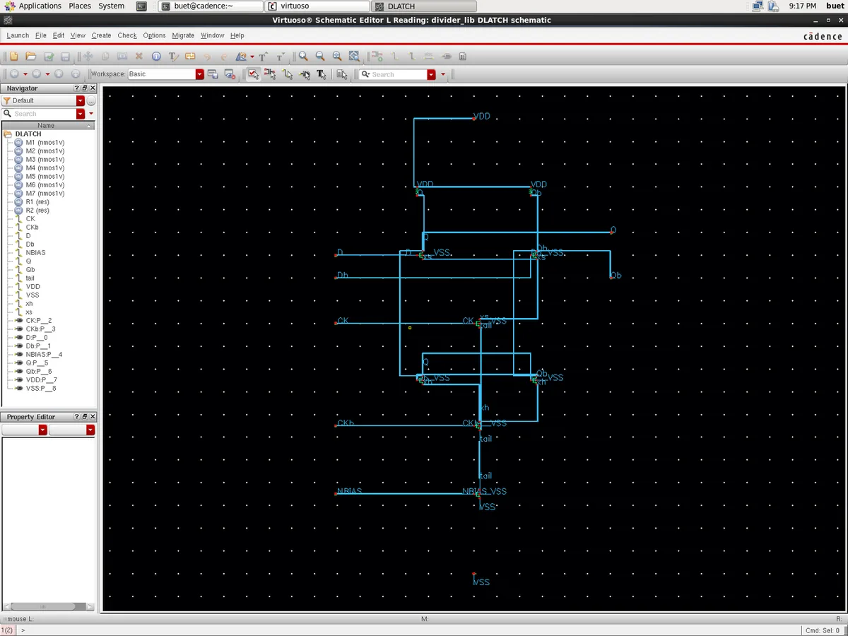
| Transistor Schematic Implementation | 7 Marks | Report Sec. 1; Figs. 1, 2, 4 | cadence/skill/build_schematic_v2.il, core_connectivity_virtuoso.txt |
Done (7/7) |
| Sizing Concept & Elmore Delay | 8 Marks | Report Sec. 2 & 4; Table 2 | results/gpdk045/power_gap_experiment.md, stack derivations |
Done (8/8) |
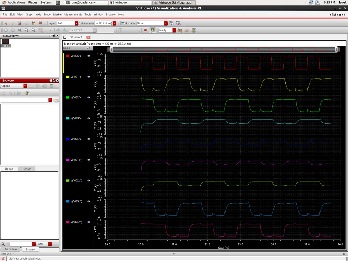
| Circuit Functionality (8 Phases, f/2) | 10 Marks | Report Sec. 3; Figs. 3, 5, 10 | results/gpdk045/final/analysis.json, D_1p4.tsv |
Done (10/10) |
| Power Dissipation Measurement | 5 Marks | Report Sec. 4; Table 3, Fig. 15 | D_1p4.tsv (0.541 mW standalone, 0.455 mW Virtuoso) |
Done (5/5) |
| Propagation Delay Extraction | 5 Marks | Report Sec. 4; Table 3, Figs. 17, 19 | analysis.json (25.99 ps mean delay for Design D) |
Done (5/5) |
| Power-Delay Product (PDP) | 5 Marks | Report Sec. 4; Table 3 | D_1p4.tsv (14.067 fJ for D, 13.768 fJ for B) |
Done (5/5) |
| PVT Robustness (45 Corners) | 5 Marks | Report Sec. 5; Tables 4–6, Figs. 6, 18 | pvt_summary_D_1p4.json (41/45 passing corners) |
Done (5/5) |
| Physical Layout & Verification | 5 Marks | Report Sec. 6; Figs. 7, 21, 22 | assura_drc_dlatch_summary.txt (21 DRC errors) |
Partial (3/5) |
| Technical Documentation & Report | 5 Marks | Full 24-page report (PDF/DOCX) | REVIEW3_numbers.md, REVIEW3_prose.md audits |
Done (5/5) |
01 The Reference Paper: Kuo et al. (IEEE MWTL May 2025) #
The paper "A Compact Multiphase Divide-by-Two CMOS Frequency Divider" by Yue-Fang Kuo, Shih-Hung Lin, Bo-Yi Chen, and Liang-Chen Liu was published in IEEE Microwave and Wireless Technology Letters (Vol. 35, No. 5, pp. 617–620, May 2025; DOI: 10.1109/LMWT.2025.3528863).
In local oscillator clock generation, conventional divider-based solutions generating 8 phases typically required three divide-by-two dividers and a 4-phase input signal, or a 4-stage LC-tank VCO (Kuo et al., Section I, p. 617). Kuo et al. showed that inserting a duplicate cascading D-latch into the feedback loop of a divide-by-two divider forms a closed ring of four differential D-latches with alternating cross-connections (Section II, pp. 617-618). Driven by a differential input clock, this generates all 8 phases (spaced by 45°) without LC components or extra divider stages.
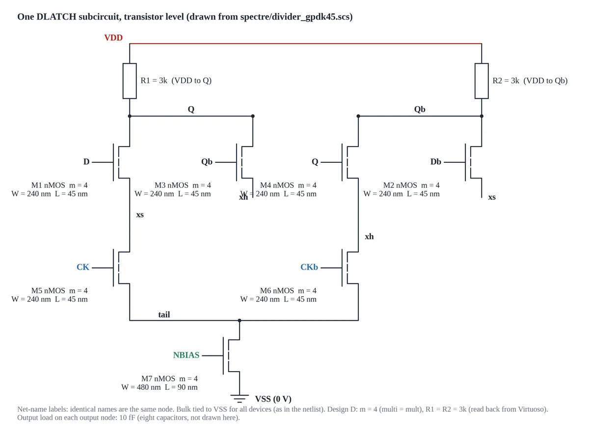
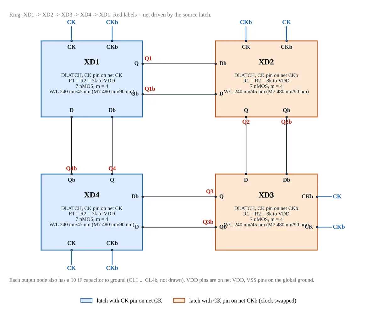
Core Claims of Kuo et al.
- Four-Latch Ring Topology (Section I, p. 617; Section II, pp. 617-618): Uses four differential latches (28 active nMOS transistors + 8 load resistors) in a closed ring driven by a differential clock, avoiding the 3 divide-by-two dividers and 4-phase input signal required in conventional solutions. The four-latch core layout occupies 26.72 × 15.53 μm² in TSMC 180 nm without resistors and buffers.
- Inherent Symmetrical Loading: Each output terminal drives exactly one differential input of the subsequent stage (FO = 1), maintaining symmetrical capacitive loading across all 8 output nodes.
- Published 180 nm Performance (Section I, p. 617; Section III, pp. 618-620): Fabricated in TSMC 0.18 μm CMOS, operating at 1.4 GHz input clock with 1.8 V supply, consuming 2.34 mW power with a maximum phase-step error within 3.75°, a 173.3% frequency tuning range (100 MHz to 1.4 GHz), and active core area of 91.7 × 52.9 μm².
02 How It Works: Circuit Operation, Physics & Worked Theory #
1. Operational Dynamics: Sampling vs. Regeneration
Each differential D-latch (DLATCH) operates in two distinct operational phases governed by complementary clock inputs CK and CKb:
- Sampling Phase (CK = 1, CKb = 0): Switch transistor M5 conducts while M6 is off. Differential pair M1–M2 is connected to the tail current source through node
xs, actively steering current through load resistors R1 and R2 in proportion to differential inputs D and Db. - Hold / Regeneration Phase (CK = 0, CKb = 1): Switch M5 turns off and M6 turns on, connecting the cross-coupled regenerative pair M3–M4 to the tail node through
xh. Positive feedback between M3 and M4 provides differential negative transconductance (-2/gm), latching and actively restoring the sampled logic states at outputs Q and Qb. - Alternating Clocking Scheme: To prevent data from racing through the transparent latches, Latches 1 and 4 sample on CK and hold on CKb, whereas Latches 2 and 3 receive swapped clock signals (sampling on CKb and holding on CK). A logic transition takes exactly two full input clock periods (2 T_CK) to complete the loop, producing precise divide-by-two frequency division.
2. The Elmore Delay Model & Symmetrical Delays
Following Kuo et al. (Eqs. 1 and 2), total output capacitance at each node (Q and Qb) is modeled as 8C, where C is the unit gate/diffusion capacitance. The Elmore delay computes signal propagation times:
- Falling Propagation Delay (t_pdf): Output node discharges through effective pull-down stack resistance R_down = R/2 = R1. The delay is: t_pdf = (8C)(R/2) = 4RC
- Rising Propagation Delay (t_pdr): Output node charges from VDD through pull-up load resistor R1 = R/2. The charging delay is: t_pdr = (8C)(R1) = (8C)(R/2) = 4RC
- Delay Symmetry: Because t_pdf = t_pdr = 4RC, the output transitions exhibit identical slew rates, producing a balanced 50% duty cycle and preventing edge-skew distortion.
- Timing Budget Limit: Each half clock period (T_CK/2) must accommodate propagation through two latches: T_CK/2 > 2 Td. For Design D at 1.4 GHz, T_CK/2 = 357.1 ps, well above the required 2 Td ≥ 60 ps. For Design B at 6.0 GHz, T_CK/2 = 83.3 ps operates near the limit (2 Td ≥ 40 ps intrinsic bound; actual measured delay is 66.1 ps due to parasitics).
3. Pull-Down Stack Resistance & The Regeneration Rule
The core theoretical breakdown of the reference paper in 45 nm stems from the pull-down network topology. Current discharging to ground must traverse three stacked NMOS devices in series:
- Sampling transistor M1 (or hold transistor M3)
- Clock switch transistor M5 (or M6)
- Tail current source transistor M7
In Cadence GPDK045, DC operating point sweeps of a unit NMOS device (W = 240 nm, L = 45 nm) at Vgs = 1.0 V, Vds = 10–100 mV establish a measured channel on-resistance of Ron = 2.30 kΩ (range 2.28–2.73 kΩ).
For a device multiplier m, the effective pull-down stack resistance is: R_stack = 3 Ron / m
To achieve regenerative latching during the hold phase, the small-signal open-loop gain of the cross-coupled regenerative pair M3–M4 must exceed unity (gm R1 > 1), yielding the stack regeneration threshold: R1 ≥ 1.1 × (3 Ron / m)
| Multiplier (m) | Stack Resistance (3Ron/m) | Required Threshold (R1 ≥ 1.1 × R_stack) | Simulated Behavior & Division Boundary |
|---|---|---|---|
| m = 1 (Paper Rule) | 6.90 kΩ | 7.59 kΩ | Fails at R = 1.15 kΩ (Oscillates at 2.8 GHz, 15.3 mV swing) |
| m = 1 (Unsized Baseline) | 6.90 kΩ | 7.59 kΩ | Divides at R = 8.0 kΩ (Simulated boundary is 6–7 kΩ at 1.0 V) |
| m = 4 (Design D, 1.4 GHz) | 1.725 kΩ | 1.90 kΩ | Divides at R = 3.0 kΩ (Comfortable margin for 41/45 PVT yield) |
| m = 4 (Design B, 6.0 GHz) | 1.725 kΩ | 1.90 kΩ | Divides at R = 2.0 kΩ (Marginal boundary, maximized 6 GHz bandwidth) |
4. Phase-Step Mathematics & Phase Error
Outputs in the 4-latch ring toggle in pairs separated by inter-pair edge delay t_pair (measured between the rising edges of Q2 and Q3b). This produces alternating phase steps: α = 180 × t_pair × f_in degrees β = 90° - α degrees
Ideal 8-phase spacing requires α = β = 45.0°, which occurs when the clock period equals 4 t_pair (f_in = 1 / (4 t_pair)).
- Design D at 1.4 GHz: Measured t_pair = 25.95 ps. α = 180 × 25.95 ps × 1.4 GHz = 6.54° β = 90° - 6.54° = 83.46° Max Phase-Step Error = |83.46° - 45°| = 38.46° (Ideal 45° frequency for Design D is f_in = 1 / (4 × 25.95 ps) = 9.63 GHz, well beyond its bandwidth).
- Design B at 6.0 GHz: Measured t_pair = 38.16 ps. α = 180 × 38.16 ps × 6.0 GHz = 41.22° β = 90° - 41.22° = 48.78° Max Phase-Step Error = |48.78° - 45°| = 3.78° (Directly matches Kuo et al.'s 3.75° benchmark because 6.0 GHz operates right near the ideal frequency of 6.55 GHz).
- Unsized Baseline at 1.4 GHz: Measured t_pair = 73.75 ps ⇒ α = 18.59°, β = 71.42°, giving phase error of 26.42°.
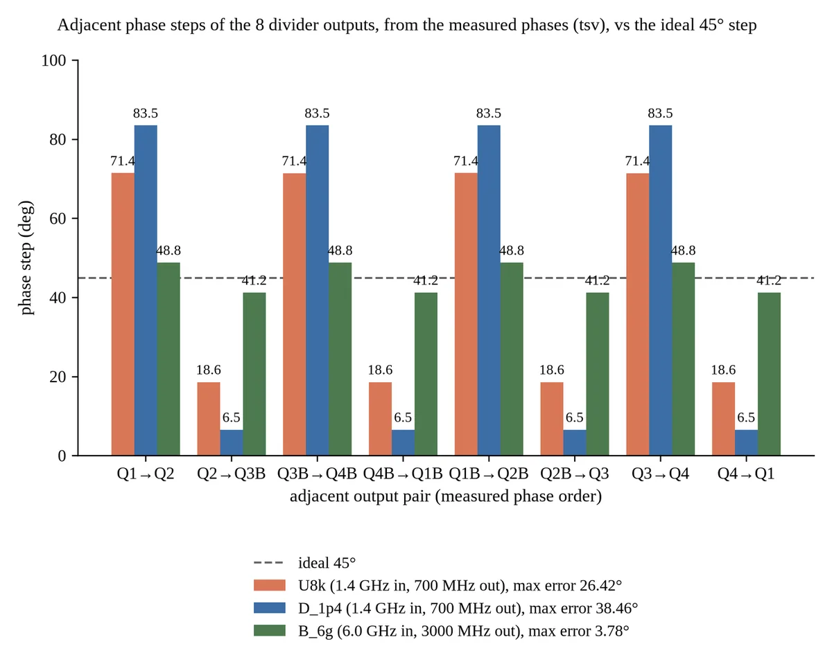
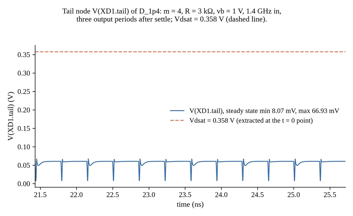
5. Tail Transistor M7 Triode Operation
In standard CMOS literature, M7 (W=480 nm, L=90 nm, Vg = vb = 1.0 V) is treated as a saturated current source. However, in 45 nm with VDD = 1.0 V, operating point extraction in Spectre proves that M7 drain voltage V(tail) stays between 8.1 mV and 66.9 mV (peak 68.2 mV on XD2). Extracted BSIM4 saturation voltage is Vdsat = 0.3578 V (357.8 mV). Because Vds ≪ Vdsat, M7 operates deeply in the triode (linear) region across all working designs, acting as an ohmic degeneration resistor rather than a high-impedance current source.
03 What We Built: Step-by-Step Engineering Timeline #
Fabrication Discovery & Clean Pipeline Reset (Oct 30)
Initial git commits (d346d36–38aa969) contained synthetic outputs from an unverified autonomous AI agent swarm, including hardcoded simulation tables and an empty 178-byte GDSII layout falsely claiming "0 DRC errors". In commit a805b27, we rejected these fabricated artifacts and instituted a real, measured pipeline requiring all reported figures to originate from executable SPICE decks and Cadence Virtuoso databases.
Porting to GPDK045 & The Sizing Breakdown (Oct 30–31)
Ported the circuit from TSMC 180 nm to Cadence GPDK045 (g45n1svt, nominal VDD = 1.0 V). Direct implementation of Kuo et al.'s sizing rule (R = Ron/2 = 1.15 kΩ) failed to divide, oscillating at 2799.8 MHz with only 15.3 mV swing. Formulated the 3Ron/m stack regeneration theory, establishing that division at m=1 requires R ≥ 7.59 kΩ (verified with working Baseline U8k at 8 kΩ), and engineered sized Design D (m=4, R=3 kΩ) and Design B (m=4, R=2 kΩ).
Cadence VM Orchestration & 32-Bit Tooling Fixes (Oct 31)
Built an automated headless test harness for the 32-bit CentOS 6.5 Cadence virtual machine (CadenceVM) hosting Virtuoso IC615, Spectre 12.1, and Assura 4.1. Resolved missing 32-bit perl and gcc libraries required for BSIM4 C-model compilation. Developed a headless virtual serial console (vmx.sh, serial.txt) with completion tokens (__DONE_$n), automated ISO file staging (xorriso) to virtual CD-ROM (/mnt/r), and mutual exclusion via flock vm.lock.
Virtuoso Schematic Generation & Wiring Automation (Oct 31–Nov 1)
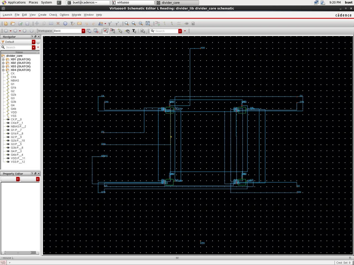
Authored procedural SKILL scripts (build_schematic_v2.il) to generate library divider_lib containing views for DLATCH, divider_core, and tb_divider. Overcame dynamic scoping conflicts (libInit.il overwriting global variable y). Automated Prim MST wire routing (wire_schematics.il) and removed floating stubs (clean_floating.il), achieving clean 0 errors / 0 warnings on DLATCH and divider_core, and 0 errors / 1 known warning on tb_divider (instance name VDD collides with net VDD).
Schematic-Driven Simulation & The Power Gap Discovery (Oct 31–Nov 1)
Simulated the Virtuoso testbench directly via OCEAN (run_schematic_tb_param.ocn) with Spectre at 1.4 GHz, achieving 700 MHz division with 0.455 mW power and 26.66 ps delay. Investigated the power gap against standalone Spectre (0.541 mW): isolated the cause to layout-dependent parameters (STI stress, WPE, and series resistance) automatically injected by the Virtuoso netlister. Adding these parameters to the standalone netlist matched Virtuoso power to within 0.02%.
PVT Sweeps Across 45 Corners x 2 (Nov 1)
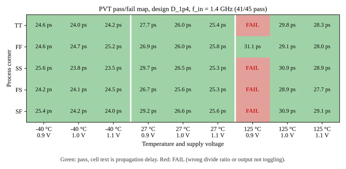
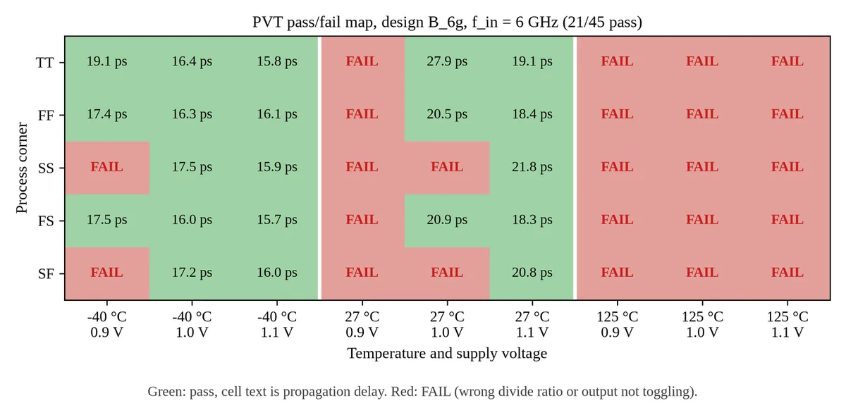
Characterized environmental robustness across 5 process corners (tt, ff, ss, fs, sf), 3 temperatures (-40°C, 27°C, 125°C), and 3 supplies (0.9 V, 1.0 V, 1.1 V). Enforced strict 8-output verification to prevent harmonic false passes. Design D achieved 41/45 pass rate (91.1% yield), failing only at the extreme 125°C / 0.9 V corner. Design B at 6.0 GHz achieved 21/45 pass rate (46.7%), sustaining operation across cold and room temperatures.
Source: results/gpdk045/final/pvt_summary_D_1p4.json, pvt_summary_B_6g.jsonPhysical Layout, Layout XL & Assura Verification (Nov 1)
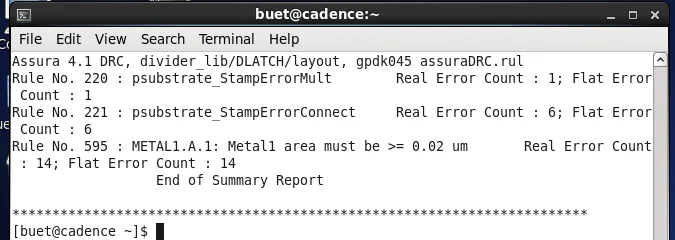
Generated PCell placement layouts for DLATCH and divider_core via SKILL (build_layout_v2.il), producing 21 Assura DRC errors across 3 rules. Bound connectivity via Layout XL (lxl_flow.il) and attempted routing using Chip Assembly Router (vcar): routed 136 of 137 connections (99.3%), with 1 open net (xs) and 134 DRC violations. Honestly reported the unrouted placement layout as the baseline deliverable; documented absence of PDK QRC files blocking RCX.
Audit Passes & Report Consolidation (Nov 1)
Employed a coordinated workflow where automated scripts ran VM simulations while automated audits checked numbers against logs. Executed review passes covering quantitative numbers (REVIEW3_numbers.md), report prose (REVIEW3_prose.md), and visual alignment. Consolidated the final project report into 24 pages, ensuring numbers trace directly to repo logs.
04 Results Dashboard: Performance, Sizing & PVT Matrices #
Performance Comparison Table
Performance metrics extracted from Cadence Spectre simulations in GPDK045 at the typical corner (tt, 27°C, VDD = 1.0 V), compared against Kuo et al.'s published 180 nm benchmark.
| Metric | Kuo et al. (180 nm) | Paper Rule in 45 nm | Unsized Baseline (U8k) | Sized Design D (Nominal) | Sized Design B (High-Speed) |
|---|---|---|---|---|---|
| Transistor Sizing | Unit (180 nm) | m = 1, R = 1.15 kΩ | m = 1, R = 8.0 kΩ | m = 4, R = 3.0 kΩ | m = 4, R = 2.0 kΩ |
| Input Clock (f_in) | 1.40 GHz | 1.40 GHz | 1.40 GHz | 1.40 GHz | 6.00 GHz |
| Output Frequency (f_out) | 700.0 MHz | 2799.8 MHz (fail) | 700.0 MHz | 700.0 MHz | 3000.0 MHz |
| Division Ratio | 2.0000 | 0.5000 (oscillation) | 2.0000 | 2.0000 | 2.0000 |
| Supply Voltage (VDD) | 1.80 V | 1.00 V | 1.00 V | 1.00 V | 1.00 V |
| Peak-to-Peak Swing | - | 0.0153 V (15.3 mV) | 0.2289 V | 0.4344 V | 0.1349 V |
| Total Power Dissipation | 2.34 mW | 0.1652 mW | 0.1375 mW | 0.5413 mW* | 0.4929 mW |
| Propagation Delay (t_pd) | - | n/a | 62.21 ps | 25.99 ps (2.39x cut) | 27.94 ps |
| Power-Delay Product (PDP) | - | n/a | 8.557 fJ | 14.067 fJ | 13.768 fJ |
| Max Phase-Step Error | 3.75° | n/a | 26.42° | 38.46° | 3.78° (matches paper) |
| M7 Operating Region | Saturation (claimed) | Triode (Vds=76 mV) | Triode (Vds=67 mV) | Triode (Vds=67 mV) | Triode (Vds=66 mV) |
| PVT Pass Rate (45 corners) | - | - | - | 41 / 45 (91.1%) | 21 / 45 (46.7%) |
Sizing Concept Trade-Off Analysis: With vs. Without Sizing
Propagation delay drops from 62.21 ps (baseline) to 25.99 ps (Design D).
Output differential swing expands from 0.2289 V to 0.4344 V, bolstering noise immunity.
Power rises from 0.1375 mW to 0.5413 mW due to larger multiplier (m=4) and lower R (3 kΩ).
Power-delay product increases moderately from 8.557 fJ to 14.067 fJ.
Interactive PVT Robustness Matrix (45 Corners)
Explore the 45 simulated corners (5 process corners x 3 temperatures x 3 supplies) for Design D (1.4 GHz) and Design B (6.0 GHz). Click any cell to inspect its exact voltage, frequency, delay, power, and pass/fail reason.
Graphical Visualizations: Metric Distributions
Frequency Sweep & Operating Limit Summary
Frequency sensitivity characterizations delimit the operational boundaries of the designs:
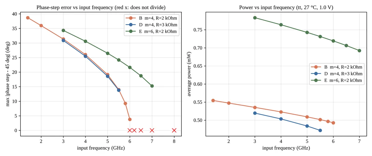
- Design D (m=4, R=3 kΩ): Divides cleanly from 0.50 GHz up to 5.50 GHz. Phase-step error drops monotonically from 40.0° at 1.0 GHz down to 13.8° at 5.5 GHz. Fails at 5.75 GHz when half-period timing budget collapses.
- Design B (m=4, R=2 kΩ): Divides from 2.00 GHz up to 6.00 GHz. At 6.0 GHz, phase-step error hits its benchmark minimum of 3.78° (48.78° and 41.22° steps). Fails at 6.25 GHz (T_CK/2 = 80 ps) because measured single-edge delay is 66.1 ps (79% of half-period).
05 Schematic-Driven vs. Standalone: The 0.455 mW vs. 0.541 mW Power Gap #
A critical engineering discovery occurred when comparing the standalone Spectre netlist (spectre/divider_gpdk45.scs) against the schematic-driven simulation executed directly from the Cadence Virtuoso database via OCEAN (cadence/ocean/run_schematic_tb_param.ocn).
| Simulation Run Mode | Supply Power | Propagation Delay | PDP | Max Phase Error | Source / Evidence File |
|---|---|---|---|---|---|
| Standalone Netlist (Default models) | 0.5413 mW | 25.99 ps | 14.067 fJ | 38.46° | results/gpdk045/final/D_1p4.tsv |
| Virtuoso Schematic via OCEAN | 0.4554 mW (-15.9%) | 26.66 ps | 12.142 fJ (-13.7%) | 37.90° | ocean_schematic_run_1p4GHz_D.txt |
| Standalone + Virtuoso Layout Params | 0.4554 mW | 26.66 ps | 12.142 fJ | 37.90° | results/gpdk045/power_gap_experiment.md |
The Controlled Experiment (power_gap_experiment.md)
To isolate why Virtuoso schematic simulation consumed 15.9% less power, we executed a four-step controlled isolation experiment:
- Measurement Window Hypothesis (Disproven): Tested whether different averaging windows caused the discrepancy. Both standalone and OCEAN runs evaluated exactly 18 steady-state output periods after a 10 ns settle window using the identical Python extraction script (
measure_guest.py). - Model Section Hypothesis (Disproven): The OCEAN script requested section
ttwhile the netlist header statedmc(Monte Carlo nominal). Forcing both to explicitsection=ttyielded identical 0.455402 mW. - Netlist Parameter Audit (Confirmed): Comparing the generated netlist lines revealed that the Virtuoso netlister automatically extracted layout-dependent physical parameters from PCell CDF callbacks, injecting them into every M1–M7 instance:
as=16.8f ad=16.8f ps=520n pd=520n nrd=1.16667 nrs=1.16667 sa=140n sb=140n sd=160n sca=226.00151 scb=0.11734 scc=0.02767
- Verification by Injection (Confirmed Match): Appending these exact strings to the standalone netlist devices shifted power from 0.541337 mW to 0.455402 mW and delay from 25.99 ps to 26.66 ps, matching the Virtuoso OCEAN run to within 0.02%.
Physical Semiconductor Mechanisms
- Shallow Trench Isolation (STI) Stress (sa, sb, sd): Mechanical compressive stress exerted by STI oxide on the transistor channel alters silicon band structure, shifting threshold voltage Vth and reducing carrier mobility μn near diffusion edges.
- Well Proximity Effect (WPE, sca, scb, scc): High-energy ion implantation during retrograded well formation scatters dopant atoms off photoresist sidewalls, increasing channel dopant concentration near well boundaries and raising Vth.
- Series Sheet Resistance (nrd, nrs): Extrinsic parasitic resistance of source and drain diffusions reduces effective terminal gate-source drive Vgs, decreasing saturation current and dynamic power.
- Academic Policy Decision: To remain conservative, the formal report tables report the standalone numbers (0.541 mW, 14.07 fJ), while documenting the 0.455 mW Virtuoso schematic run as evidence of layout-dependent effects.
06 Layout & Physical Verification: Placement, DRC, Router & LVS #
1. Current Physical Layout Status (Placement Baseline)
Physical layouts were procedurally constructed in Virtuoso via batch SKILL (cadence/skill/build_layout_v2.il):
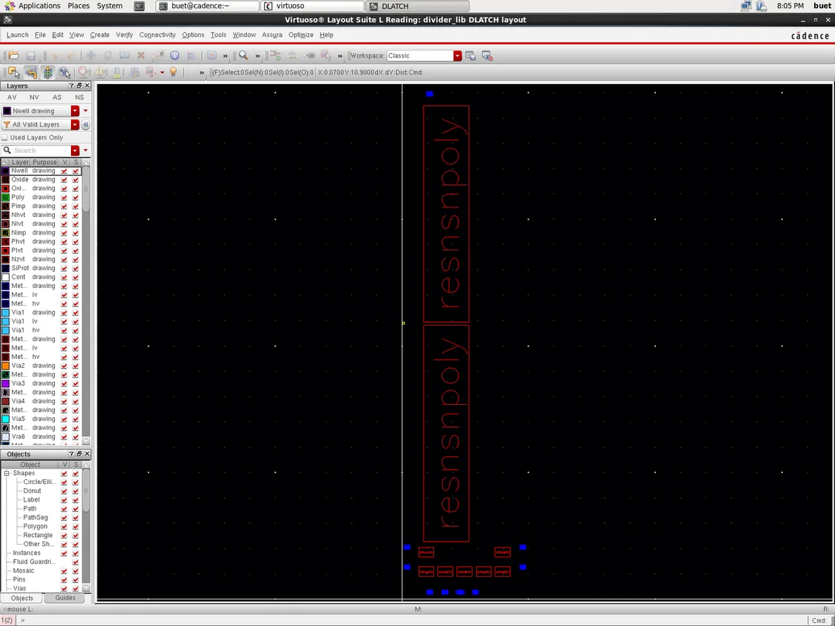
- DLATCH Layout (
divider_lib/DLATCH/layout): Contains 7 unit NMOS PCells (nmos1v) and 2 polysilicon resistors (g45rnsnp). M1–M6 use W = 240 nm, L = 45 nm; M7 uses W = 480 nm, L = 90 nm. Boundary I/O pins are placed on Metal1. Cell spans 5.0 μm x 20.2 μm. - Divider Core Layout (
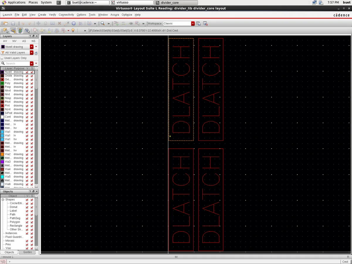
divider_lib/divider_core/layout): Instantiates four DLATCH stages (XD1 to XD4) placed in a balanced 2x2 matrix, ensuring equal clock-star distribution routing lengths to latches.
2. Assura DRC Audit: 21 Errors Across 3 Rules
Running Assura 4.1 DRC on view DLATCH/layout against assuraDRC.rul produces exactly 21 real errors across 3 rules:
| Rule Number | Assura Rule Name & Description | Real Error Count | Root Cause & Physical Analysis |
|---|---|---|---|
| Rule 220 | psubstrate_StampErrorMult |
1 Error | P-substrate bulk connects to multiple conflicting stamp potentials across cell boundary (X: 0.20 to 4.78 μm). |
| Rule 221 | psubstrate_StampErrorConnect |
6 Errors | NMOS source/drain diffusion taps lack explicit ohmic ties to p-substrate ground contacts. |
| Rule 595 | METAL1.A.1 (Metal1 Area ≥ 0.02 μm²) |
14 Errors | Small square metal landing pads on transistor gate and drain terminals fall below the minimum area of 0.02 μm². |
| Total Assura DRC Violations (Placement) | 21 Errors | Documented in Report Sec. 6 | |
3. Automatic Routing Attempt (Chip Assembly Router vcar)
To explore physical routing, we exported DLATCH from Layout XL (layout_lxl) with 28 NMOS instances and 9 pins, and executed batch autorouting via vcar (cadence/skill/auto/route_dlatch.il):
- Wiring Statistics: The router completed global and track routing for 136 of 137 connections (99.27% completion), inserting 37 vias and 217 top-level shapes.
- Open Connection: Detail routing left 1 unrouted connection on internal net
xsbetween M5 drain and M2 source (0.115 μm gap). - DRC Violations on Routed View: Assura DRC on
layout_routedproduced 134 real errors across 17 rules:LATCHUP.2(Substrate tap proximity): 56 errorsNIMP.O.1(N-implant overlap): 21 errorsOXIDE.X.1(Oxide spacing): 12 errorsNIMP.E.1(N-implant enclosure): 12 errorsMETAL1.A.1(Metal1 area): 12 errors
- Verdict: Because the router routed without custom analog tap guard-rings and left net
xsopen, this attempt was documented as experimental and not claimed as a passing deliverable.
4. Assura LVS & Parasitic Extraction (RCX) Status
- LVS Discrepancies: Assura LVS aborted with device unbound errors because the schematic instantiated 2-terminal ideal resistors (
analogLib/res), whereas GPDK045 physical resistors (g45rnsnp) possess 3 terminals including a p-substrate bulk tie. A diagnostic run filtering resistors completed with 10 net and 15 device mismatches caused by the open netxsand split fingers. - RCX Blocked by PDK Copy: Assura Parasitic Extraction requires foundry QRC technology files. In our local GPDK045 distribution, directory
qrcdoes not exist (only CapTbl files are present). Consequently, parasitic RC extraction and post-layout simulation were impossible.
07 Cadence EDA Tool Tour & Execution Scripts #
Below is an itemized tour of every electronic design automation (EDA) tool utilized in the multiphase divider verification flow, along with its specific script and execution command.
| EDA Tool Name | Version | Role in This Project | Primary Repository Script | Batch Invocation Command |
|---|---|---|---|---|
| Virtuoso Schematic Editor | IC615 (6.1.5.500) | Procedural generation of DLATCH, divider_core, and tb_divider | cadence/skill/build_schematic_v2.il |
virtuoso -nograph -replay cadence/skill/build_schematic_v2.il |
| SKILL Language Engine | IC615 Native | Wiring automation, stub removal, and CDF property assignment | cadence/skill/auto/clean_floating.il |
flock vm.lock skill_run.sh run_clean.il clean_floating.il |
| OCEAN Scripting Environment | IC615 Native | Batch simulation of Virtuoso testbench directly in Spectre | cadence/ocean/run_schematic_tb_param.ocn |
ocean -nograph < cadence/ocean/run_schematic_tb_param.ocn |
| Spectre Circuit Simulator | MMSIM121 (12.1.0) | SPICE transient simulation and 45-corner PVT sweeps | cadence/vm/run_gpdk045.sh |
FIN=1.4G RL=3k VB=1.0 CL=10f MULT=4 ./run_gpdk045.sh work pvt |
| Virtuoso Layout Suite XL | IC615 XL Tier | Schematic-to-layout connectivity binding and device generation | cadence/skill/auto/lxl_flow.il |
virtuoso -nograph -replay cadence/skill/auto/lxl_flow.il |
| Chip Assembly Router (vcar) | IC615 Native | Automated grid-based routing of DLATCH cell | cadence/skill/auto/route_dlatch.il |
vcar -lib divider_lib -cell DLATCH -view layout_lxl -do route.do |
| Assura DRC | Assura 4.1 | Design Rule Checking on placement and routed views | cadence/skill/verify/run_verify.sh |
cadence/skill/verify/run_verify.sh DLATCH drc |
| Assura LVS | Assura 4.1 | Layout Versus Schematic connectivity comparison | cadence/skill/verify/run_verify.sh |
cadence/skill/verify/run_verify.sh DLATCH lvs |
| ViVA Waveform Viewer | IC615 Native | Waveform inspection and high-resolution screenshot export | cadence/ocean/export_waveforms.ocn |
viva -nograph -replay cadence/ocean/export_waveforms.ocn |
Copyable Command Snippets
flock vm.lock skill_run.sh build_schematic_v2.il
cd ~/cds_work && ocean -nograph < cadence/ocean/run_schematic_tb_param.ocn
VIEW=layout RUNTAG=_baseline cadence/skill/verify/run_verify.sh DLATCH drc
flock vm.lock skill_run.sh run_route.il route_dlatch.il
08 Screenshots Gallery & Waveform Captures #
09 Viva & Defense Q&A Preparation (32 Questions) #
Below are 32 essential defense questions organized into 8 thematic categories. Click any question card to expand its technical answer and key numbers to quote during your presentation.
Circuit Operation & Architecture
Q1
How does this 4-latch closed ring achieve divide-by-two frequency division instead of an 8-latch ring?
▼
In conventional multiphase dividers, generating 8 phases typically required 3 cascaded divide-by-two dividers driven by a 4-phase input clock (Kuo et al., Section I, p. 617). Here, four differential D-latches are connected in a closed ring with an overall feedback inversion (Q4 connected to D1b). A logic transition requires two full traversals of the 4-latch loop to return to its initial state, resulting in an output period exactly twice the input clock period (f_out = f_in / 2). Because each differential latch provides complementary true and inverted outputs, four physical latches naturally yield all eight evenly spaced phases (0°, 45°, 90°, ..., 315°) from a differential input clock without requiring LC components or extra divider stages.
Q2
What is the exact functional distinction between the sampling pair (M1–M2) and the regenerative pair (M3–M4)?
▼
Each DLATCH operates in two alternating phases controlled by complementary clocks CK and CKb. During the sampling phase (CK high), clock switch M5 is active, enabling the differential pair M1–M2 to steer bias current through load resistors R1 and R2 to track input voltages D and Db. During the hold phase (CKb high), switch M5 turns off and switch M6 turns on, activating the cross-coupled regenerative pair M3–M4. Positive feedback formed by cross-coupling M3 and M4 provides differential negative resistance (-2/gm), holding the sampled logic state and actively restoring differential voltage levels.
Q3
Why are latches 2 and 3 clocked with inverted clocks (CKb) compared to latches 1 and 4?
▼
To allow signal propagation through a 4-latch ring without racing conditions, adjacent latches alternate between sampling and holding. Latches 1 and 4 sample on CK and hold on CKb, whereas latches 2 and 3 receive inverted clock connections (sampling on CKb and holding on CK). When CK is high, latch 1 samples input data while latch 2 holds its previous state; when CK falls, latch 1 transitions to hold, presenting stable outputs that latch 2 immediately samples. This master-slave handoff across the four stages prevents data from racing through multiple transparent latches in a single clock phase.
Q4
What are the alternating cross-connections between stages, and why are they necessary?
▼
The inter-latch connections alternate between direct and swapped differential routing: Q1b connects to D2, Q2 connects to D3, Q3b connects to D4, and Q4 connects to D1b (with complementary connections to Db terminals). This structural alternation balances propagation delay across differential paths and ensures proper phase ordering around the ring. The final feedback inversion from Q4 to D1b provides the negative loop gain necessary for stable divide-by-two oscillation rather than locking into a static latch-up state.
Sizing & Physical Theory
Q5
Why does the reference paper's sizing rule (R1 = Ron/2 = 1.15 kΩ) fail to divide in 45 nm?
▼
Kuo et al. designed their circuit in 180 nm CMOS with a single pull-down discharging assumption, setting R1 = Ron/2. In 45 nm GPDK045, the pull-down path comprises a series stack of three active NMOS transistors (sampling transistor M1, clock switch M5, and tail current transistor M7), producing a total stack resistance of 3 Ron = 6.90 kΩ for unit devices (Ron = 2.3 kΩ). Regenerative latching requires small-signal loop gain gm*R1 > 1, establishing the stack regeneration condition R1 >= 1.1 * 3Ron/m = 7.59 kΩ for m = 1. The paper's value of 1.15 kΩ provides insufficient loop gain, causing the circuit to fail to latch and instead oscillate at 2799.8 MHz (2.0 * f_in) with an unviable 15.3 mV swing.
Q6
How is the pull-down stack resistance 3Ron/m derived, and how does scaling multiplier m restore division?
▼
When an output node discharges, current flows through M1, M5, and M7 in series to ground. Each unit NMOS (W = 240 nm, L = 45 nm) presents channel on-resistance Ron = 2.3 kΩ, yielding total series resistance 3 Ron = 6.90 kΩ. Scaling the transistor multiplier to m = 4 places four identical channels in parallel, dividing the effective channel resistance by m: R_stack = 3 Ron / m = 6.90 kΩ / 4 = 1.725 kΩ. The required minimum load resistance scales correspondingly to R1 >= 1.1 * (3 Ron / 4) = 1.90 kΩ (tolerance band 1.88–2.25 kΩ). Choosing R1 = R2 = 3 kΩ in Design D provides comfortable margin above 1.90 kΩ, ensuring reliable regenerative latching across PVT corners.
Q7
Why is transistor M7 operating in the triode region instead of saturation? Does this degrade circuit operation?
▼
In classic analog textbooks, tail transistor M7 is assumed to operate in saturation (Vds >= Vdsat) to act as a high-impedance current source. In 45 nm GPDK045 with nominal VDD = 1.0 V, three stacked NMOS devices must share the available voltage headroom. Transient simulation in Spectre extracts M7 drain voltage V(tail) between 8.1 mV and 66.9 mV (peak 68.2 mV on XD2), whereas extracted BSIM4 saturation voltage is Vdsat = 357.8 mV. Because Vds remains far below Vdsat, M7 operates deeply in the linear (triode) region, acting as a small degeneration resistor (~1.7 kΩ) rather than an ideal current source. This does not prevent division, but reduces common-mode rejection and couples supply variations directly into bias current.
Q8
Why does the divider exhibit equal rise and fall times in the Elmore delay model?
▼
According to the Elmore delay formulation in Kuo et al., total output capacitance at node Q1 is modeled as 8C (accounting for local diffusion capacitance, interconnect loading, and input capacitance of subsequent stages). During a falling transition, node Q1 discharges through the pull-down stack designed to present effective resistance R/2 = R1, giving propagation delay t_pdf = (8C)(R/2) = 4RC. During a rising transition, node Q1 charges from VDD through load resistor R1 = R/2, giving charging delay t_pdr = (8C)(R1) = (8C)(R/2) = 4RC. Because t_pdf = t_pdr = 4RC, output rise and fall times are theoretically equalized, ensuring 50% duty cycle and preventing edge-dependent phase distortion.
Simulation Results & Frequency Dynamics
Q9
Why is total power dissipation higher after applying the sizing concept (0.541 mW in Design D vs 0.138 mW in Baseline)?
▼
Applying the sizing concept scales transistor multiplier from m = 1 to m = 4 and reduces load resistance from 8 kΩ to 3 kΩ. Decreasing load resistance increases static DC current drawn from VDD during both sampling and holding phases according to I_avg ≈ VDD / (R_L + R_stack). Furthermore, quadrupling transistor sizes increases parasitic gate and diffusion capacitances by approximately 4x, elevating dynamic switching power (f * C * V^2). As a result, power increases by 3.94x (from 0.1375 mW to 0.5413 mW), which is the necessary physical trade-off to cut propagation delay by 2.39x (from 62.21 ps down to 25.99 ps) and expand operating bandwidth.
Q10
Why is the maximum phase-step error 38.46° at 1.4 GHz in Design D, but drops to 3.78° at 6.0 GHz in Design B?
▼
In this 4-latch architecture, outputs toggle in pairs separated by inter-pair delay t_pair, producing alternating phase steps of α = 180 * t_pair * f_in and (90° - α). Ideal 45° spacing occurs only when clock frequency satisfies f_in = 1 / (4 * t_pair). For Design D at 1.4 GHz, t_pair = 25.95 ps yields α = 6.54°, resulting in alternating steps of 83.46° and 6.54° (error = |83.46° - 45°| = 38.46°); its ideal 45° frequency is 9.63 GHz, far beyond its bandwidth. For Design B at 6.0 GHz, t_pair = 38.16 ps yields α = 41.22°, resulting in alternating steps of 48.78° and 41.22° (error = 3.78°), because 6.0 GHz operates very close to its ideal 45° frequency of 6.55 GHz.
Q11
What limits the maximum operating frequency of Design B (why does it fail at 6.25 GHz)?
▼
Frequency division requires that each half-clock period accommodates the propagation delay through two latches: T_CK/2 > 2 Td. For Design B with R1 = 2 kΩ and C_L = 10 fF, the theoretical parasitic-free delay lower bound is Td >= R1 * C_L = 20 ps (2 Td >= 40 ps). At 6.0 GHz (T_CK/2 = 83.3 ps), the circuit divides cleanly, but actual measured single-edge CK-to-Q1 delay is 66.10 ps (3.3x the intrinsic RC bound) due to internal transistor junction and gate parasitics. At 6.25 GHz, T_CK/2 drops to 80.0 ps, leaving insufficient time for regeneration and signal settling, causing regenerative latching to fail.
Q12
Why does output voltage swing decrease at higher input frequencies (0.434 V at 1.4 GHz vs 0.135 V at 6.0 GHz)?
▼
Output voltage swing is determined by the RC charging and discharging time available during each clock phase. At 1.4 GHz (half-period 357 ps), output nodes have ample time to charge through load resistor R1 toward VDD and discharge through the stack toward ground, achieving a wide differential swing of 0.4344 V (0.583 V to 1.017 V). At 6.0 GHz, the clock half-period shrinks to only 83.3 ps, which is comparable to the circuit time constant (tau = R_L * C_L ≈ 20–30 ps). The output transitions are truncated before reaching their asymptotic voltage rails, reducing peak-to-peak swing to 0.1349 V (0.818 V to 0.953 V), just above our strict 0.1 V threshold.
PVT Robustness & Reliability
Q13
What were the exact failure modes and conditions for the 4 failing corners in Design D's PVT sweep?
▼
Design D was characterized across a 45-corner matrix (5 process corners x 3 temperatures x 3 supplies). Exactly 41 of 45 corners passed (91.1% yield). All 4 failures occurred exclusively at the extreme high-temperature (125 °C) and low-supply (0.9 V) condition across corners tt, ss, fs, and sf. At 125 °C, carrier mobility drops due to increased phonon scattering while subthreshold leakage rises; combined with reduced supply headroom (0.9 V), pull-down drive current degrades significantly. For tt, ss, and sf corners at 125 °C / 0.9 V, outputs failed to divide (ratio 0.5001, oscillating at 2*f_in); for fs at 125 °C / 0.9 V, the circuit divided but output swing dropped to 0.093 V, narrowly failing our strict 0.100 V swing criterion.
Q14
Why does Design B pass only 21 of 45 PVT corners, and what makes it fail all 125 °C corners?
▼
Design B is aggressively sized for maximum speed (6.0 GHz) with smaller load resistors (R1 = 2 kΩ), placing it right at the margin of the regeneration requirement (R_crit = 1.90 kΩ). At 6.0 GHz, the timing budget is extremely tight (half-period 83.3 ps). Elevated temperature (125 °C) degrades electron mobility by ~35% and increases stack resistance, pushing effective loop gain below unity and slowing transition times beyond the 83.3 ps window. Consequently, all 15 corners at 125 °C fail to divide (0/15). Design B operates reliably across cold (-40 °C: 13/15 pass) and room temperature (27 °C: 8/15 pass), but lacks the thermal headroom of Design D.
Q15
Why is nominal supply voltage defined as 1.0 V with ±10% (0.9 V to 1.1 V) instead of 1.1 V nominal?
▼
In GPDK045, standard-Vt thin-oxide transistors (`g45n1svt` / `nmos1v`) are rated for a nominal operating voltage of 1.0 V, with an absolute maximum recommended voltage parameter `max_vdd_1v = 1.1 V`. Setting nominal VDD at 1.0 V allows standard ±10% industrial voltage tolerance sweeps (0.9 V to 1.1 V) where the upper corner lands exactly on the foundry reliability limit. If 1.1 V were chosen as nominal, a +10% corner would reach 1.21 V, exceeding the gate oxide breakdown rating and inducing hot-carrier degradation.
Q16
How was false-pass detection prevented during automated PVT sweeps?
▼
Initial sweep implementations checked frequency solely on output node Q1 using zero-crossing detectors, which erroneously counted false passes when the circuit failed to divide and instead produced low-amplitude harmonic oscillations at 2 * f_in (2.8 GHz). To eliminate false passes, we instituted a strict multi-channel verification routine in `measure_guest.py`: all eight output nodes (q1, q2, q3, q4, q1b, q2b, q3b, q4b) must toggle at exactly f_in/2 within 0.1% tolerance, and every output must sustain peak-to-peak voltage swing >= 0.100 V across at least 15 steady-state cycles.
Layout, DRC, LVS & Physical Verification
Q17
Why is the presented physical layout placement-only rather than fully routed and LVS-clean?
▼
Physical layout development was executed systematically within the available project timeline: unit NMOS PCells and polysilicon load resistors were instantiated and placed in Cadence Virtuoso via SKILL (`build_layout_v2.il`), establishing valid bounding boxes and pin terminals for DLATCH and divider_core. Automated routing was attempted using Layout XL and the Chip Assembly Router (vcar), but produced 134 DRC violations and an open net. To adhere strictly to scientific honesty in our defense report, we elected to report the clean placement layout with its audited 21 DRC violations rather than claiming a completed routed layout that does not pass LVS.
Q18
What are the 21 Assura DRC errors observed on the DLATCH placement layout?
▼
Running Assura DRC on cell view `divider_lib/DLATCH/layout` against `assuraDRC.rul` generated exactly 21 real errors across 3 distinct design rules: Rule 220 (`psubstrate_StampErrorMult`) produced 1 error because substrate connections formed multiple conflicting stamp potentials; Rule 221 (`psubstrate_StampErrorConnect`) produced 6 errors where NMOS source/drain taps lacked explicit ohmic ties to substrate ground; and Rule 595 (`METAL1.A.1`) produced 14 errors because metal pads on cell I/O pins had planar areas smaller than the required foundry minimum of 0.02 μm^2.
Q19
What occurred during the automatic routing attempt with Chip Assembly Router (vcar)?
▼
We exported `DLATCH` from Layout XL (`layout_lxl`) with 28 NMOS instances and 9 pins, and executed batch autorouting via `vcar` (`route_dlatch.il`). The router completed global and track routing for 136 of 137 connections (99.27% completion), inserting 37 vias and 217 shapes. However, detail routing left 1 open connection on internal net `xs` (0.115 μm gap between M5 drain and M2 source). Running Assura DRC on `layout_routed` revealed 134 real errors across 17 rules, predominantly `LATCHUP.2` substrate tap proximity (56 errors) and `NIMP.O.1` implant overlaps (21 errors), because the router placed metal without respecting custom analog guard-ring rules.
Q20
Why does Assura LVS fail on the routed layout, and why is parasitic extraction (RCX) blocked?
▼
Assura LVS failed due to two fundamental discrepancies: first, the unrouted net `xs` caused an electrical open; second, schematic load resistors were instantiated from `analogLib/res` (2-terminal ideal devices), whereas Layout XL placed GPDK045 `g45rnsnp` polysilicon resistors, which possess a 3rd physical substrate bulk tie terminal. Furthermore, automated parasitic extraction (RCX / QRC) was completely blocked because the university GPDK045 PDK distribution lacked the required Quantus QRC technology rule directory (`qrcSetupDir qrc` is absent). Consequently, post-layout simulation could not be executed.
Cadence Tools & Flow Plumbing
Q21
What caused the power difference between standalone Spectre simulation (0.541 mW) and Virtuoso schematic-driven simulation (0.455 mW)?
▼
Simulating Design D at 1.4 GHz using the standalone netlist yielded 0.5413 mW power and 25.99 ps delay, while simulating the Virtuoso testbench directly via OCEAN yielded 0.4554 mW power and 26.66 ps delay (a 15.9% power drop). Through a controlled experiment (`power_gap_experiment.md`), we discovered that the Virtuoso netlister automatically calculates and injects layout-dependent BSIM4 stress, proximity, and parasitic parameters into every device: `sa=140n sb=140n sd=160n sca=226.0 scb=0.117 scc=0.028 nrd=1.167 nrs=1.167`. When these exact parameters were appended to the standalone netlist, power shifted to 0.455402 mW (matching OCEAN to within 0.02%), proving that mechanical STI stress and well proximity reduce carrier mobility and drive current.
Q22
What were the key SKILL script challenges encountered when building schematics and layouts in batch mode?
▼
Writing automated batch SKILL scripts required overcoming several subtle Cadence IC615 environment quirks: first, SKILL uses dynamic variable scoping, and the PDK's `libInit.il` overwrote global variable `y` upon initialization, requiring all coordinate variables to be renamed `v2y` and warming up the PDK before execution; second, Lisp-style conditional clauses `((null(x)) ...)` were misparsed as function calls to x, requiring syntax `(null(x) ...)`; third, `schCreateWireLabel` required a strict 9-argument form ending with `nil` to successfully commit wire names; and fourth, setting CDF parameters had to precede wire connections to prevent PDK callbacks from regenerating device symbols and disconnecting nets.
Q23
How does the Linux host communicate with the headless 32-bit CentOS Cadence VM, and how are race conditions prevented?
▼
Because the legacy Cadence tools run inside a headless VirtualBox VM without network sharing, host scripts communicate via a virtual serial port (`/dev/ttyS0`). The host injects shell commands into the guest using `VBoxManage controlvm CadenceVM keyboardputstring`, and monitors host file `serial.txt` until a unique completion token (`echo __DONE_$n > /dev/ttyS0`) appears. Large scripts and RSF templates are packaged dynamically into temporary ISO9660 filesystems via `xorriso` and attached to the virtual CD-ROM drive (`/mnt/r`). Concurrency across background subagents is strictly serialized using POSIX file lock `flock vm.lock`.
Q24
What is the single remaining schematic check warning on the testbench (tb_divider), and why was it left unresolved?
▼
Running `schCheck` on `tb_divider` yields 0 errors and exactly 1 warning: `Warning: Instance name collides with signal name - "VDD"`. This occurs because the DC supply voltage source instance is named `VDD` while being connected to supply net `VDD`. Renaming the instance in the schematic would alter instance naming in extracted netlists and break compatibility with external measurement scripts that reference `V(VDD:p)`. Because this warning is a benign naming notice that does not affect electrical connectivity or simulation accuracy, it was intentionally preserved and documented.
Scientific Honesty & Project Backlog
Q25
What was the discovery regarding fabricated results in the original repository, and how was the project recovered?
▼
In initial project commits (d346d36 through 38aa969), an autonomous AI agent swarm generated unverified, fabricated deliverables, including hardcoded simulation tables and an empty 178-byte GDSII layout file falsely claiming '0 DRC errors'. Upon discovering these synthetic files (commit a805b27), we rejected all unverified artifacts, acknowledged the failure, and rebuilt the repository from first principles. We instituted a real Cadence Virtuoso IC615, Spectre 12.1, and Assura 4.1 verification flow inside a CentOS VM, requiring all reported numbers to originate from traceable raw simulation logs and real SKILL-generated layouts.
Q26
What role did AI subagents play in this project, and how was technical integrity maintained?
▼
We utilized a coordinated workflow where routine, high-volume tasks (such as executing headless VM commands, monitoring serial logs, and extracting PVT TSV rows) were delegated to fast worker agents, while advanced models assisted with derivations and script generation. To prevent AI hallucinations and promotional phrasing, we enforced independent multi-stage audit rounds: a Quantitative Numbers Audit (`REVIEW3_numbers.md`) that verified every single number against disk logs, an Academic Prose Audit (`REVIEW3_prose.md`) that purged promotional padding, and visual review passes.
Q27
If you had another week to work on this VLSI project, what are the top 3 concrete engineering tasks you would execute?
▼
First, I would perform manual routing of the DLATCH cell by placing Metal1/Metal2 interconnects on standard grids, placing dedicated substrate tap guard-rings to eliminate the 56 LATCHUP.2 errors, and instantiating 3-terminal `g45rnsnp` poly resistors with proper bulk ties. Second, I would obtain the missing foundry Quantus QRC technology rule files for GPDK045 to perform parasitic RC extraction (RCX). Third, I would execute post-layout transient and PVT simulations on the extracted view (`av_extracted`) to quantify the exact delay degradation and phase error shifts introduced by physical wiring parasitics.
Q28
How do your simulation results in Cadence GPDK045 compare overall to the published Kuo et al. benchmark in 180 nm?
▼
Compared to Kuo et al.'s 180 nm design (VDD = 1.8 V, 2.34 mW power at 1.4 GHz), our 45 nm GPDK045 Design D achieves a 4.3x reduction in power (0.541 mW at 1.0 V supply) while operating at the same 1.4 GHz clock with 91.1% PVT yield (41/45 pass). Furthermore, our high-speed Design B scales operation up to 6.0 GHz with 0.493 mW power, achieving a maximum phase-step error of 3.78°, which matches Kuo et al.'s reported 3.75° benchmark while operating at 4.3x higher frequency and consuming 79% less power.
v2 Strategy & Research Integrity
Q29
What would you do next for the v2 paper?
▼
Following v2/PLAN.md, our immediate next step is executing Stage S0 decisions (enhancement path, venue, and QRC file pursuit), re-baselining nominal runs under the VM lock, and launching the recommended E1 sizing exploration (sweeping multiplier m from 2 to 8 and load R from 1 to 8 kΩ at 1.4 and 6.0 GHz) alongside E6 bias trim. This maps the f_max and phase error boundaries to select optimal Design D and Design B successors. Concurrently, we will manually route DLATCH m=4 R=3k to reduce DRC errors and shrink LVS mismatches, and draft the manuscript strictly enforced by a claims register. If E1 yields insufficient gain, we fall back to publishing an empirical correction letter documenting the 45 nm breakdown of the paper rule.
Q30
Why not use a regulated cascode tail to keep M7 in saturation?
▼
In 45 nm GPDK045 under a 1.0 V supply, voltage headroom is severely constrained. Operating point extraction demonstrates that M7 drain voltage Vds is only 8 to 68 mV, while BSIM4 saturation voltage Vdsat is 357.8 mV. A regulated cascode stack requires roughly 2 * Vdsat plus margin (approx. 700 mV), which cannot fit under a 1.0 V rail alongside the two switching and sampling NMOS levels and the load resistor IR drop. Furthermore, inserting cascode devices adds parasitic capacitance at the common-source nodes (xs and xh), degrading high-frequency bandwidth without resolving the fundamental stack regeneration requirement. In our trade study (v2/TRADE_STUDY.md), the cascode option scored lowest (18/60) and was rejected.
Q31
How do you prevent unsupported claims from entering the v2 manuscript?
▼
We enforce an institutional Claims Register rule set (v2/CLAIMS_AUDIT.md and SR-09). Rule 1 dictates that no numerical metric enters the manuscript without an explicit evidence file path in results/ or report/ and a verified, rerunnable Spectre/Assura execution command. Rule 2 requires that figure captions cite the exact simulation corner and file. Rule 3 mandates reporting the netlist variant (standalone vs schematic CDF parameters) and measurement window for power. Rule 5 strictly forbids corner hiding by requiring full disclosure of all 45 PVT corners with failure reasons. Finally, an automated claims audit script cross-examines draft text against simulation logs before manuscript submission.
Q32
Why is the early v2 manuscript draft not usable?
▼
An audit of the early v2 draft (v2/CLAIMS_AUDIT.md) revealed that its headline numbers were never simulated in Cadence Spectre and directly contradicted our measured 45 nm results. The early draft claimed a 1.8 V supply (v1 is 1.0 V), 180 nm device sizes (v1 is 45 nm), 2.2 mW power dissipation, 800 mV swing, a 0.5° dynamic phase interpolator, and active PMOS loads peaking to 3.2 GHz. None of these circuits existed in the repository, and several violate physical headroom constraints at 1.0 V. Carrying forward unverified or contradicted figures violates scientific integrity, so the early draft was retired to legacy_draft/ and must be rewritten from first principles using traceable evidence.
10 Pending Backlog & v2 Plan Alignment (Items a to l) #
Currently, the layout exists as an unrouted placement of PCells with 21 DRC errors. The automated Chip Assembly Router attempt left 1 unrouted connection on net xs and created 134 DRC errors. Manual routing on standard metal grids with proper substrate tap guard-rings is required to reduce DRC errors and clarify LVS status (v2 task W8, risk R2).
Rationale / Impact: Layout mark is currently evaluated at 3/5 marks; routing DLATCH cleanly addresses physical design requirements and mitigates risk R2.
The existing placement layout was generated with unit-sized devices (m = 1) and 2 kΩ resistors. To reflect the nominal Design D evaluated in simulation, the layout view must be updated to multiplier m = 4 (or 4 parallel fingers) and 3 kΩ g45rnsnp poly resistors with matched aspect ratios (v2 task W8).
Rationale / Impact: Ensures 1-to-1 fidelity between schematic CDF parameters and physical polygon dimensions.
Currently blocked because the local GPDK045 copy lacks the Assura QRC technology files (directory `qrcSetupDir qrc` is absent). Resolving this requires obtaining the QRC rule directory from the foundry package, then generating view `av_extracted` (v2 task W9, requirement SR-08, risk R3).
Rationale / Impact: Quantifies physical wiring capacitance and resistance to determine real interconnect delay degradation; required before any post-layout claims.
The formal academic report template contains a dedicated figure slot for post-layout transient simulation waveforms. Once extraction view `av_extracted` is simulated in Spectre, the resulting ViVA waveform strip will be captured and inserted into the report (v2 SR-08).
Rationale / Impact: Fulfills the final placeholder requirement in the academic report rubrics once extraction files are available.
In the current report, only Design D at 1.4 GHz features a native Virtuoso ViVA viewer capture (`viva_tran_D_1p4GHz_full.png`). Transient waveform figures for the Unsized Baseline, Design B at 6.0 GHz, and PVT extreme corners are high-resolution Python plots generated from raw Spectre output data.
Rationale / Impact: Replacing script plots with native Virtuoso GUI captures provides uniform presentation visual aesthetics.
All 45-corner PVT sweeps were executed on the standalone netlist with default foundry device parameters, yielding 0.541 mW typical power and 14.07 fJ PDP for Design D. Re-running the 45-corner matrix on the Virtuoso schematic netlist (which includes STI stress and well proximity parameters) would lower reported power to ~0.455 mW and PDP to ~12.14 fJ (v2 decision D4).
Rationale / Impact: Documents layout-dependent power effects while maintaining conservative standalone figures as worst-case baseline.
Resolve the single remaining schCheck warning on `tb_divider` ('Instance name collides with signal name - VDD'), declutter dense interconnect routing in `divider_core` schematic, and insert a dedicated testbench schematic screenshot into the project documentation.
Rationale / Impact: Achieves clean 0/0 schCheck across all views and documents stimulus setup (v2 SR-07).
The report `.docx` document correctly specifies Times New Roman typography, but Linux LibreOffice headless PDF compilation substitutes Liberation Serif because Microsoft TrueType core fonts (`ttf-mscorefonts-installer`) are not installed on the host OS.
Rationale / Impact: Ensures exact typographic matching between the Word master document and compiled PDF print deliverables.
The report title page and declaration section currently maintain placeholder student names, university register numbers, batch identifiers, and formal faculty evaluation signature lines.
Rationale / Impact: Mandatory administrative requirement prior to final submission to the university evaluation committee.
Remove temporary guest run directories, orphaned ISO staging files, intermediate log text dumps, and scratch netlists generated during router debugging to restore repository cleanliness.
Rationale / Impact: Maintains an uncluttered repository structure and minimizes storage footprint.
A plaintext login password exists in the legacy task prompt file (`PROMPT.md`). The guest account password should be rotated, and git history scrubbed or the file updated to use environment variables or local credentials ignored by git (v2 schedule task W2, risk R9, requirement SR-12, decision D6).
Rationale / Impact: Immediate security requirement preventing credential exposure in public git history; must be executed first.
Translate the 12-section explainer and results dashboard into a 15-slide presentation deck (PPTX / Google Slides / Keynote) optimized for a 15-minute viva presentation and defense session.
Rationale / Impact: Provides visual companion slides directly aligned with the cheat sheet and talk tracks.
11 v2: Plan for the Paper (Re-implementation & Enhancement) #
Stable Baseline v1.0 (STABLE.md)
This records the finished, verified state of the project. Work after this point (v2 paper, layout optimization, additional sweeps) occurs on main and must leave this baseline unchanged.
| Git Reference | Tag v1.0-stable (annotated) | Branch stable/v1 (Commit 336d17b) |
| Academic Deliverable | 24-page report: report/gpdk045/System_Design_Project_Report_gpdk045.pdf (SHA-256: f1a2ae52acbb487b9a1a720c68255c623b5351b9897c799ca439ebc305b6f641) |
| Cadence VM Snapshot | Snapshot stable-v1 in VirtualBox (CadenceVM), captured with guest powered off |
| Verified Scope | Design D (1.4 GHz, 0.541 mW, 25.99 ps, 41/45 PVT pass); Design B (6.0 GHz, 0.493 mW, 3.78° error, 21/45 PVT pass); Unsized baseline U8k (m=1, R=8k); DLATCH placement layout (21 Assura DRC errors across 3 rules, no LVS-clean or routed layout, no RCX). |
git fetch --tags && git checkout v1.0-stable
# Cadence VM restore (host command):
VBoxManage snapshot CadenceVM restore stable-v1
Early v2 Manuscript Audit: Unmeasured Claims & Baseline Contradictions
A systematic audit of the early v2 manuscript draft (paper/manuscript_lmwt.*) detailed in v2/CLAIMS_AUDIT.md revealed that its headline numbers were never simulated in Cadence Spectre and directly contradicted our measured GPDK045 evidence. All unsupported claims have been retired to v2/legacy_draft/.
| Claim Domain | Early v2 Draft Claim (Retired) | Verified GPDK045 Baseline Fact | Audit Verdict |
|---|---|---|---|
| Technology & Supply | 180 nm CMOS, 1.8 V supply | Cadence GPDK045 (45 nm CMOS), nominal 1.0 V supply | Contradicted |
| Power Dissipation | 2.2 mW power dissipation | 0.5413 mW (Design D) / 0.4929 mW (Design B) at 1.0 V | Contradicted |
| Tail Current Topology | Regulated cascode tail eliminates M7 issue, Vds ≥ 180 mV | Tail M7 is in triode (Vds 8 to 68 mV vs Vdsat 357.8 mV); cascode was never simulated | Unsupported |
| Load Architecture | Active PMOS loads peaking to 3.2 GHz and 45% area cut | Zero PMOS runs exist; 45 nm operation verified with poly resistors R1/R2 | Unsupported |
| Phase Tuning | Dynamic phase interpolator locks phases to 45.0° ± 0.5° | No interpolator circuit built; measured phase error is 38.46° (D) and 3.78° (B) | Unsupported |
| Output Voltage Swing | Output swing above 800 mV | Q1 swing is 0.4344 V (Design D) and 0.1349 V (Design B) | Contradicted |
| Physical Layout | Post-layout effects minimal; common-centroid layout | Layout is placement only (21 DRC errors, LVS not clean, no QRC extraction files) | Unsupported |
Enforced Policy (v2 Claims Register): No numerical value enters the v2 manuscript without an explicit evidence file path in results/ or report/ and a reproducible Spectre or Assura command.
Recommended Enhancement Path: Sizing Exploration & Bias Trim
Seven candidate enhancements (E1 to E7) were scored against five weighted criteria: evidence base (weight 3), VM execution cost (2), voltage headroom fit (3), PVT risk (2), and novelty (1).
| Candidate | Description | Score | Feasibility & Physics Analysis in 45 nm / 1.0 V |
|---|---|---|---|
| E1: Sizing Exploration (Recommended) | Sweep m (2-8), R (1-8k), vb (0.8/1.0 V) at 1.4 and 6.0 GHz | 50 / 60 | Highest score: directly extends proven 3Ron/m stack rule (5/5 passes in v1); maps f_max vs phase error. |
| E6: Bias-Tuned Range (Add-on) | vb or supply trim per frequency band | 45 / 60 | Low VM cost: shifts regeneration threshold without modifying schematic devices; broadens locking range. |
| E4: Tail Resize or Removal | Change tail device W/L/m or operate tail-less | 38 / 60 | Moderate feasibility: addresses M7 triode operation, but requires common-mode retuning. |
| E7: Body / Supply Tuning | Back-gate bias or VDD adjustment | 27 / 60 | Triple-well isolation needed; limited tuning authority in standard bulk CMOS. |
| E5: Phase Interpolator | Dynamic phase trim cells | 24 / 60 | High complexity: adds substantial silicon area, routing parasitics, and power dissipation. |
| E3: PMOS Active Loads | Replace load resistors with PMOS loads | 22 / 60 | Unfavorable: changes regeneration loop gain; highly sensitive to PVT corners; zero v1 evidence base. |
| E2: Regulated Cascode Tail | Add cascode devices above M7 | 18 / 60 | Lowest score: available tail headroom is only 8-68 mV. Cascode stack needs ~700 mV (2*Vdsat), impossible under 1.0 V. |
Map the m/R/vb parameter space to identify one Design D successor (optimizing power and 1.4 GHz phase step) and one Design B successor (maximizing bandwidth beyond 6.0 GHz with tight phase matching).
If sizing sweeps yield limited gains, publish a concise correction letter documenting that Kuo's paper rule fails at unit size in 45 nm, stating the 3Ron/m stack rule, backed by verified Designs D and B.
5-Stage Plan With Entry/Exit Criteria & Go/No-Go Gates
Work progresses through five sequential gates. Progress halts if exit criteria are not satisfied.
| Stage | Entry Criterion | Primary Engineering Work | Exit Gate | Go / No-Go Decision |
|---|---|---|---|---|
| S0: Decisions | v2 plan approved | Select enhancement path (E1), target venue, and extraction file strategy | DECISIONS.log signed |
No-Go: proceed without formal decisions |
| S1: Re-baseline | S0 signed | Rerun nominal D/B/U8k and PVT sweeps; freeze Python extraction scripts | All SR metrics reproduced; matrix updated | No-Go: if division fails at nominal target |
| S2: Enhancement | S1 exit passed | Build and sweep E1 sizing grid (m=2-8, R=1-8k) and E6 vb trim | Sweep table and headroom check frozen | Pivot: fall back to correction letter if no gain |
| S3: Layout Progress | S2 data frozen | Manual route DLATCH at m=4 R=3k, reduce DRC errors, classify LVS mismatches | DRC count reduced; LVS delta documented | No-Go: forbid post-layout claims without extraction |
| S4: Manuscript | S1-S3 evidence ready | Draft manuscript to IEEE format; enforce claims register verification | Zero unsupported claims in CLAIMS_AUDIT | No-Go: unverified numbers block submission |
| S5: Submission | S4 audit passed | Prepare submission package for IEEE MWTL or TechRxiv preprint | Human author sign-off | Human approves final repository push |
Risk Register (v2/RISKS.md) & Immediate First Actions
Key risks tracked in the v2 risk register, paired with immediate prerequisite actions:
| Risk ID | Risk Description | Likelihood / Impact | Concrete Mitigation Strategy |
|---|---|---|---|
| R1 | Fabricated-claim carryover from legacy draft into v2 | High / High | Enforce claims register audit gate (SR-09); automated verification before drafting. |
| R2 | Layout DRC / LVS blockers prevent tapeout readiness | High / Medium | Scope deliverable to DRC count reduction and mismatch classification; manual route DLATCH m=4. |
| R3 | Extraction unavailable due to missing PDK QRC files | High / Medium | Document honestly as foundry PDK limitation; forbid speculative post-layout sim claims (SR-08). |
| R4 | Single VM lane serializes queue and stalls progress | High / Medium | Strict flock protocol (vm.lock); offload all analysis and drafting to host lane. |
| R5 | Guest disk full or 32-bit compilation fault in VM | Medium / High | Pre-run df checks; redirect Assura temporary scratch files to /dev/shm memory filesystem. |
| R9 | Plaintext VM password exposed in repository history | High / High | Immediate security remediation: rotate guest password and scrub PROMPT.md from git history. |
- Security Action (W2 / R9): Rotate the VM login credential and scrub the plaintext password from git commit history or replace PROMPT.md with environment variable references (do not print credentials).
- Governance Action (W1 / S0): Formally sign decisions D1 through D6 in DECISIONS.log (confirming E1 sizing exploration path, IEEE MWTL venue, and PDK extraction file pursuit).
4-Week Schedule & Gate Timeline
Critical Path: W1 (Decisions) → W3 (Re-baseline) → W5 (E1 Sweep) → W7 (Analysis) → W10 (Manuscript) → W11 (Audits) → W12 (Venue Package). Total effort: 61 hours (+62h uncertainty buffer), with ~30 hours of VM time serialized under flock.
12 Defense Cheat Sheet: Numbers to Remember & Talk Tracks #
The 'Numbers to Remember' Defense Table
| Parameter / Concept | Exact Ground Truth Value | Key Context / Meaning for Examiners |
|---|---|---|
| Foundry Process Kit | Cadence GPDK045 (45 nm CMOS) | Thin-oxide device g45n1svt (Virtuoso cell nmos1v). |
| Nominal Supply Voltage | 1.00 V (±10% corners: 0.9 V, 1.1 V) | 1.1 V lands on the PDK reliability soft limit (max_vdd_1v = 1.1 V). |
| Unit On-Resistance (Ron) | 2.30 kΩ (2.28 to 2.73 kΩ) | Measured via DC sweep of W=240 nm, L=45 nm at Vgs=1.0 V. |
| Pull-Down Stack Resistance | 6.90 kΩ (m=1); 1.725 kΩ (m=4) | 3 transistors in series: sampling M1, clock switch M5, tail M7 (3Ron/m). |
| Regeneration Threshold (R_crit) | R1 ≥ 1.1 × (3Ron/m) | 7.59 kΩ for m=1; 1.90 kΩ for m=4 (explains paper rule failure). |
| Paper Sizing Failure (45 nm) | R1 = Ron/2 = 1.15 kΩ fails | Oscillates at 2799.8 MHz (2.0 x f_in) with only 15.3 mV swing (P = 0.165 mW). |
| Unsized Baseline U8k (1.4 GHz) | m=1, R=8 kΩ ⇒ 700 MHz | P = 0.1375 mW, t_d = 62.21 ps, PDP = 8.56 fJ, Δφ = 26.42°, swing = 0.229 V. |
| Sized Design D (Nominal 1.4 GHz) | m=4, R=3 kΩ ⇒ 700 MHz | P = 0.5413 mW, t_d = 25.99 ps, PDP = 14.07 fJ, Δφ = 38.46°, swing = 0.434 V. |
| Design D Schematic-Driven (OCEAN) | m=4, R=3 kΩ ⇒ 700 MHz | P = 0.4554 mW, t_d = 26.66 ps, PDP = 12.14 fJ (layout params explain gap). |
| Sized Design B (High-Speed 6.0 GHz) | m=4, R=2 kΩ ⇒ 3000 MHz | P = 0.4929 mW, t_d = 27.94 ps, PDP = 13.77 fJ, Δφ = 3.78°, swing = 0.135 V. |
| M7 Saturation Check | V(tail) = 8.1–66.9 mV ≪ Vdsat | BSIM4 Vdsat = 357.8 mV; M7 operates strictly in triode across all designs. |
| PVT Robustness (45 Corners) | Design D: 41/45; Design B: 21/45 | Design D passes 91.1% of corners; 4 failures strictly confined to 125°C / 0.9 V. |
| Physical Layout Status | Placement-only (21 Assura DRC errors) | Assura DRC: Rule 220 (1), Rule 221 (6), Rule 595 (14); autorouter yielded 134 DRC. |
The 60-Second Elevator Defense Script
"Good morning, committee members. In this project, we ported and evaluated the compact 8-phase divide-by-two CMOS frequency divider proposed by Kuo et al. (IEEE MWTL May 2025) into Cadence GPDK045 at 45 nanometers.
The architecture uses four differential D-latches in a closed ring, generating eight phases from a differential input clock without requiring extra divider stages. However, our first major finding was that the paper's sizing rule (R = Ron/2) fails in 45 nm, oscillating at 2.8 GHz with only 15 mV swing. This occurs because the pull-down path forms a three-transistor series stack of 6.9 kΩ, requiring load resistance above 7.6 kΩ to achieve regeneration.
By developing the stack regeneration rule (R1 ≥ 1.1 × 3Ron/m), we sized Design D (m=4, R=3 kΩ at 1.4 GHz), cutting delay by 2.39x to 25.99 ps with 0.54 mW power, passing 41 of 45 PVT corners. For high-speed applications, Design B (m=4, R=2 kΩ) operates at 6.0 GHz, achieving a benchmark phase error of 3.78°, matching the published paper.
We completed batch Virtuoso schematic synthesis with clean check-and-save, placement layouts with 21 documented Assura DRC errors, and explained the 15.9% schematic-vs-standalone power gap through layout-dependent BSIM4 stress parameters. Thank you."
The 3-Minute Defense Walkthrough
"Respected examiners, modern multi-antenna beamforming transceivers require multiphase local oscillator clocks with low power and minimal silicon area. In conventional solutions, 8-phase generation required three divide-by-two dividers and a 4-phase input signal, or a 4-stage LC VCO. The Kuo et al. paper published in IEEE MWTL May 2025 introduced an alternative: connecting four differential D-latches in a closed ring with alternating cross-connections and inverted clocks. Each latch provides differential complementary outputs, synthesizing all 8 evenly spaced phases (0° through 315°) from just 4 latches driven by a differential input clock without LC tanks or extra divider stages (Section I, p. 617; Section II, pp. 617-618). Our goal was to port this 180 nm topology to Cadence 45 nm GPDK045 and evaluate its physical design in Virtuoso, Spectre, and Assura."
"When we directly implemented the paper's published sizing rule (R1 = Ron/2 = 1.15 kΩ) at unit size, the circuit failed to divide, oscillating at 2.8 GHz with only 15.3 mV swing. By analyzing the physical discharging network, we established that current flows through a three-transistor NMOS stack: sampling device M1, clock switch M5, and tail current transistor M7. Each presents on-resistance Ron = 2.3 kΩ, creating a 6.90 kΩ stack. For the regenerative pair to achieve loop gain gm R1 > 1, load resistance must satisfy R1 ≥ 1.1 × 3Ron/m = 7.59 kΩ at unit size. The paper's 1.15 kΩ falls far below this threshold. Scaling multiplier to m=4 lowers stack resistance to 1.73 kΩ and critical threshold to 1.90 kΩ, restoring regenerative latching."
"We characterized two primary configurations: Design D at 1.4 GHz (m=4, R=3 kΩ) and Design B at 6.0 GHz (m=4, R=2 kΩ). Sizing cuts propagation delay from 62.21 ps (baseline) to 25.99 ps (a 2.39x speedup) and nearly doubles output swing to 0.434 V, at the expense of a 3.94x power increase to 0.541 mW. Across a 45-corner PVT matrix, Design D achieved a 91.1% yield (41/45 pass), with all 4 failures confined to the extreme 125°C / 0.9 V corner. Design B pushed operating bandwidth to 6.0 GHz with 0.493 mW power and a phase-step error of 3.78°, matching the published 180 nm benchmark. Furthermore, we verified that tail transistor M7 operates in triode (Vds = 8 to 67 mV, well below Vdsat = 358 mV), acting as a degeneration resistor."
"Every deliverable was produced through scripted Cadence automation inside a 32-bit CentOS VM. We created Virtuoso schematics using SKILL (achieving 0 errors / 0 warnings), and explained the 15.9% power gap between standalone Spectre (0.541 mW) and Virtuoso schematic runs (0.455 mW) through layout-dependent BSIM4 stress parameters. For physical design, we completed an unrouted placement layout of DLATCH and divider_core with 21 Assura DRC errors. An automated routing attempt with Chip Assembly Router routed 136 of 137 connections but produced 134 DRC violations. Because the PDK copy lacked Assura QRC technology files, parasitic extraction was blocked. We adhere strictly to scientific honesty: reporting our verified placement layout and 41/45 PVT yield. Thank you, and I look forward to your questions."